SK hynix and SanDisk Release the First HBF Standard: NAND Memory Built for AI Inference
SanDisk and SK hynix released the first HBF specification through OCP: a NAND memory tier between HBM and SSDs, up to 512GB and 3.0 TB/s for AI inference.
News Report

What happened
On August 4, 2026, SanDisk and SK hynix published the first technical specification for High Bandwidth Flash (HBF), a NAND-based memory type meant to sit between the fast, expensive memory bonded to AI accelerators and the slower storage below it. The document was released through the Open Compute Project (OCP), the industry body that standardizes server and rack hardware for the large cloud operators, and it landed alongside the Future of Memory and Storage (FMS) conference running August 4 to 6 at the Santa Clara Convention Center.
The two companies started working together on HBF in August 2025 and formed a consortium around it in February 2026. This week's release turns that year of work into an actual standard other vendors can design against.
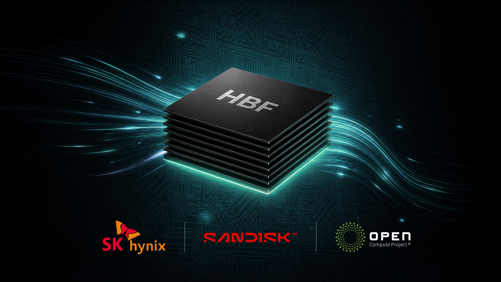
The memory wall HBF is aimed at
Modern AI inference is limited less by raw compute than by how much fast memory sits next to the chip. High Bandwidth Memory (HBM), the DRAM stacks bonded to GPUs, delivers the bandwidth but tops out at modest capacity and carries a steep price. Below it, SSDs are cheap and enormous but far too slow to feed an accelerator directly. The gap between those two tiers is where large models spend a lot of their time waiting.
HBF is the answer SK hynix and SanDisk are proposing for that gap. It stacks NAND flash the way HBM stacks DRAM, trading some speed for a large jump in capacity. SK hynix says a single HBF stack can hold roughly 8 to 16 times the capacity of an HBM stack while still moving data at bandwidths in HBM's range. For inference that needs to keep enormous key-value caches or model weights close to the compute, that trade can matter more than peak DRAM speed.
Inside the first HBF spec
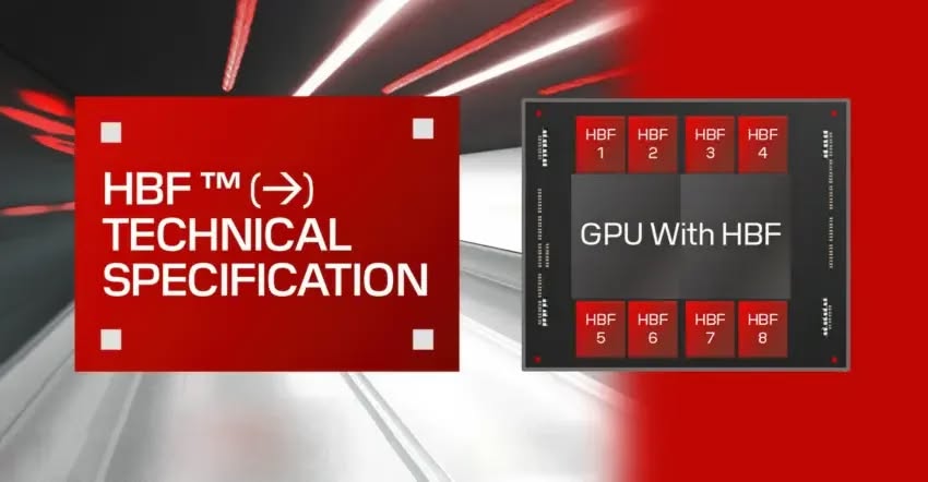
The initial specification is specific about the numbers. It defines two stack configurations, an 8-high and a 16-high arrangement of NAND dies, reaching up to 512GB per stack. Bandwidth comes in three grades, running from about 0.4 terabytes per second at the low end to 3.0 TB/s at the top. A designer picks the grade that fits the power and cost envelope of the system.
For the connection to the processor, the spec adopts UCIe (Universal Chiplet Interconnect Express), the open die-to-die interconnect that a growing number of chiplet designs already use. That choice lets an HBF stack talk to a CPU or GPU over an interface silicon designers do not have to invent from scratch.
Beyond the headline figures, the document lays out the xPU-to-HBF host interface, electrical guidelines, reliability and packaging guidance for the die stack, expected performance, and a software user guide covering read and write operations. It is enough for a system architect to start designing around HBF rather than reading a marketing slide.
Why an open OCP standard matters
Publishing through OCP is the part worth watching. HBM has been effectively controlled by a handful of memory makers, and its capacity ceiling and pricing have become a real constraint on AI hardware. Releasing HBF as an open specification invites more than one supplier to build compatible parts and lets accelerator designers plan for it without betting on a single vendor.
The workstream behind the standard already reaches past the two memory companies. Google and Tenstorrent are named participants, with SanDisk and SK hynix as the primary contributors. The spec is also written so HBF can coexist with HBM on the same system rather than replace it, which is how the companies expect it to be used: HBM for the hottest data, HBF for the large pool behind it.
Alper Ilkbahar, SanDisk's chief technology officer, framed it around cost per token. The specification, he said, gives system designers "a practical path to bring high-capacity, high-bandwidth memory closer to compute" and is aimed at "AI systems built to improve token economics at scale." Kim Chun-sung, who heads solution development at SK hynix, put it more broadly, arguing that the spread of AI means "overall data processing structures must be redesigned."

What SK hynix showed at FMS 2026
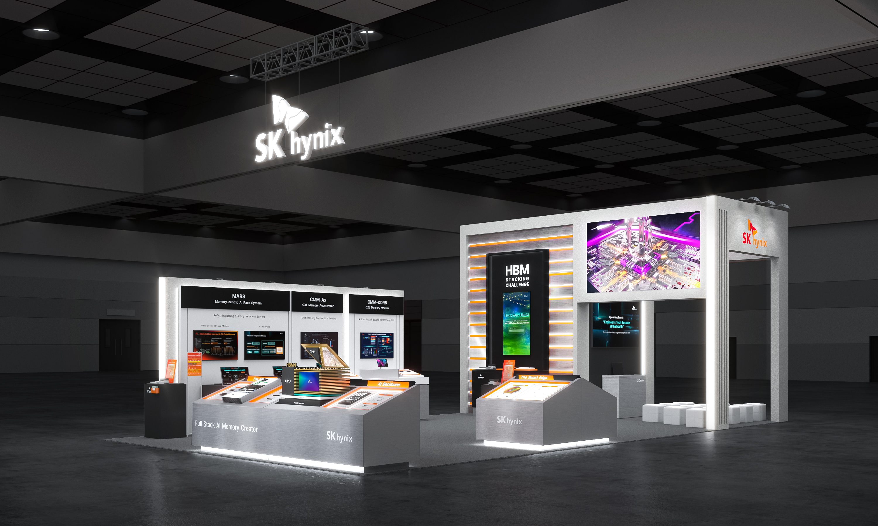
HBF was not the only thing on the SK hynix stand. The company used FMS 2026 to reveal its V10 375-layer 4D NAND, which it says delivers about 2.5 times the power efficiency of the previous generation and is headed for mass production in early 2027 in high-capacity enterprise SSDs. That NAND is the kind of building block HBF stacks will eventually be made from.
The companies also put HBF on the conference program directly. An August 4 keynote from SK hynix executives Kim Chun-sung and Kang Uk-song carried the title "Orchestrating Efficient AI Infrastructure through Tiered Memory," and a panel on August 6 brought SK hynix, SanDisk, and Google DeepMind together under the heading "Breaking the Memory Wall with High Bandwidth Flash."
What's next
A specification is a starting line, not a shipping product. The August 2026 release tells designers what HBF will look like; as of August 2026 it does not put a single part in a server. SK hynix has sketched an architecture it calls H3, in which HBM and HBF share an interposer next to a GPU and an address router inside the HBM base die splits requests between the two. That is a design proposal, not a product on a price list.
The near-term signals to watch are whether a third memory supplier commits to the standard, whether the major accelerator vendors design HBF interfaces into upcoming chips, and how the real-world bandwidth and endurance of a NAND-based tier hold up under constant inference traffic. If those fall into place, HBF becomes a genuine third rung in the AI memory hierarchy. If they do not, it stays an elegant answer to a problem the market solved another way. Either way, an open standard with Google and Tenstorrent already at the table is a more serious start than most memory concepts get.
Read the original source
Head to the original source for the full announcement and complete details.
Read Original Source